Semiconductor Scaling Shifts to Packaging, Photonics and AI
- Gate
- AI & ML
- Departs
- Crew
- Gregory Haley
- Passengers
- 979
Chip demand is rising faster than expected. Meeting it now depends on integrating, testing and manufacturing whole systems, with AI taking on more engineering work.

The semiconductor industry has reached the revenue milestone it once expected to hit in 2030. The harder question now is whether its factories and engineering methods can keep pace with demand. At SEMICON West 2026 in San Francisco, more than 30,000 attendees and a sold-out exhibit floor gathered around a shift in emphasis: progress increasingly depends on how well chips, memory, packaging, optics, power and software work together.
SEMI President and CEO Ajit Manocha projected a market exceeding $2 trillion by 2030, with a possible $3 trillion by 2035. The association also forecast $149 billion in spending on 300mm fab equipment this year, rising to $227 billion by 2029. Construction is due to begin on 20 new 300mm fabs or production lines in 2026.
AI infrastructure accounts for much of the expansion, while electrification, autonomous vehicles, robotics and industrial automation add demand of their own. The strain comes from the growing complexity of the systems these chips must serve. Adding compute creates pressure on memory bandwidth, power delivery and cooling; placing memory closer to processors can cut data movement while concentrating heat. Splitting a large die into smaller components can improve yield and let each function use a suitable process, but it adds interfaces that must be connected, powered, cooled and tested.
“We’ve started talking about how to re-engineer engineering because you need to co-design and optimize across multiple intersections,” said Sassine Ghazi, president and CEO of Synopsys. He described a design problem spanning physics, materials, process technology, architecture, software and the model defining the workload. His point captures the industry’s new scaling challenge: individual components still matter, but their interactions increasingly determine system performance.

Packaging becomes part of the architecture
Advanced packaging is moving from the end of the chip development process to the beginning of system design. It determines how compute, memory and interconnects fit together, and affects power, cooling, performance and manufacturing yield.
“Packaging is no longer simply the place where semiconductor innovation ends,” said Lalitha Immaneni, vice president of semiconductor R&D at Intel Foundry. “Increasingly, it’s the place where system innovation begins.” She argued that teams must optimize across silicon, packaging and the platform, rather than treat each part as a separate task.
Nitin Deshpande, Marvell’s vice president of advanced packaging, made a similar case at imec’s pre-show ITF USA program. “The package is really becoming a system where the compute, the memory, the interconnects, the power, the cooling, all of these things come together.”
Designing that system is only one hurdle. The assembly still needs to work at high volume, with reliable processes, sufficient yield and costs customers can support. Deshpande warned that promising concepts have little commercial value if suppliers cannot deliver the parts on time or repeat the process at scale.
That gap also changes what “scaling” means. Patrick Vandenameele, CEO of imec, observed that data centers can add accelerators and racks to increase capacity, but that growth differs from traditional semiconductor scaling. “These data centers are true engineering marvels,” he said. “But at the same time, this is not what we semiconductor people call scaling. It looks a little bit more like multiplication.” The distinction is useful: adding hardware can grow total capacity, while improving a chip system requires coordinated advances in the parts and their connections.
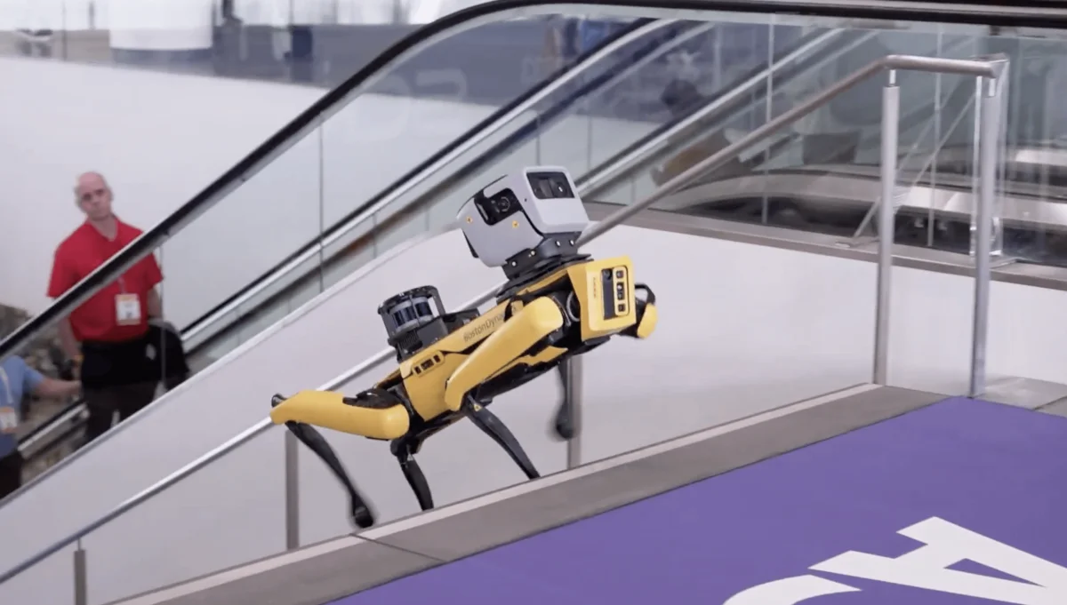
Fig. 2: Redefining a system. Source: SEMI
AI moves from answering questions to pursuing outcomes
AI has been used for years in chip design, process control and defect classification. Generative systems made it easier to query tools and data in natural language. The next step discussed at the show was agentic AI: software that receives an objective and can call tools, models or other agents to work toward it.
“We started from an assistant copilot to generative capability to now what we’re describing as long-horizon autonomous agents, where instead of giving a prompt, you give an outcome,” Ghazi said.
The appeal is tied to the size of modern engineering problems. A recipe for a Lam Research etcher can have a potential search space on the order of 1023 possibilities, according to David Fried, Lam’s chief AI officer and corporate vice president of Semiverse Solutions. That number describes a space too large for engineers to explore manually. Fried said AI can work across the many interacting parameters and specifications that shape a process.
Finding a pattern and acting on it are different steps. An AI system that flags an unusual process signature is doing something different from one that changes a recipe. A prediction of equipment degradation also raises a separate question from an automated decision to stop production.
Ghazi said Synopsys already has customer projects in which agents can take a specification through verified RTL, a process that traditionally required several engineers and months. People still set the architecture and review the result before manufacturing. Even so, the example shows that AI is starting to take on work inside established engineering flows, rather than simply making information easier to find.
For manufacturers, the open questions are practical: Which decisions can an agent make on its own? What physical models and process limits constrain its choices? What evidence should teams require before an automated action affects production? AI is already part of semiconductor design and manufacturing. The next measure of its influence will be how much authority engineers let it exercise.

Fig. 3: What comes next is an evolving topic of great interest to a lot of people. Source: SEMI
Packaging needs evidence at every step
Advanced packaging has moved beyond proving that different kinds of chips can be combined. The challenge is to assemble them repeatedly and economically while avoiding the loss of valuable components when a later step reveals a defect. That pressure is extending the idea of a “known-good” part beyond the die.
Intel fellow Ravi Mahajan, director of substrate and advanced packaging pathfinding at Intel Foundry, said the company sorts even passive bridges, which contain metal lines, before they enter a package. The aim is to start with the best available evidence about each component and confirm the assembled package as thoroughly as possible. “Known-good” is an aspiration, he cautioned, because no inspection can establish certainty about every possible defect. Manufacturers can add test features to improve coverage and reduce uncertainty.
ASE follows a similar approach. In some fan-out processes, teams can test the interconnect structure before attaching active silicon. “Everything we do, every layer, we have the ability to confirm that it is good before we put on the most expensive part,” said Yin Chang, ASE’s executive vice president.
Some combinations of silicon and high-bandwidth memory can represent as much as $30,000 in value, Chang said. ASE uses automated optical inspection and X-ray extensively, with AI helping identify subtle differences in assemblies that can include as many as half a million joints. The goal is to catch problems before more value is added, because scrapping an expensive assembly is costly.
Inspection cannot catch everything at the earliest opportunity. Bonding introduces new interfaces, and heat, pressure and material interactions can change an assembly after its components have passed inspection. Some defects become visible only after another process step. Manufacturers therefore have to decide how much uncertainty they can carry into each stage, and where additional inspection is worth its time and cost.
Test and inspection follow the assembly
Testing is also changing as optics joins advanced packages. Electrical test typically compares a device’s response against an expected result. Optical devices can have a range of acceptable responses, and teams need to connect those measurements to possible defects. Co-packaged optics adds physical constraints: package size, weight, density and connector geometry all affect how equipment reaches the device.
Amkor senior director of manufacturing test technology Vineet Pancholi said customers want outsourced assembly and test providers to handle electrical and optical probing on both sides of a package efficiently. The basic sequence of probing, burn-in, final test and system-level test remains in place, he said, but newly designed optical tests are expected to take longer at first. Test times may fall as fabrication and assembly processes mature.
When a fault appears late, manufacturing teams also need information about earlier steps. Reiner Fenske, CEO of Microtronic, described retaining wafer images so teams can compare process stages and narrow down where a defect began. Keeping that history can matter more than inspection speed, he said; archived lot data and images may help diagnose an issue months after production.
This makes test less like a final pass-or-fail checkpoint and more like a running record of evidence. Wafer results, inspection images, assembly history and earlier test insertions can guide later checks or help identify process drift. Traceability becomes harder as a die moves from its original wafer coordinates through reconstructed wafers, panels and multi-die packages. AI may help find patterns across those records, but only if each data point remains connected to the correct device and process history.
Co-packaged optics meets the factory
Optics is moving closer to compute because electrical links face rising power and signal-integrity demands as bandwidth and distance increase. That shift, from pluggable optical modules toward near-package and co-packaged designs, makes optical integration more directly a manufacturing challenge.
Huan Ma, a senior technologist at Intel Foundry, said precision bonding must control alignment in all six degrees of freedom while meeting semiconductor manufacturing requirements for throughput, automation and standardized material handling. Materials must also hold alignment through assembly, reflow and reliability stresses.
Inspection needs to measure the optical features that predict performance. Ma pointed to geometry, angles and positions that affect insertion loss and coupling efficiency. His argument is that working optics alone won’t establish a production process; packaging must make those optical elements repeatable at scale.
Other companies raised related hurdles. EV Group discussed the metrology and throughput demands of measuring multiple alignment points across hundreds of dies in die-to-wafer integration. Lam Research covered waveguide fabrication, modulator materials and fiber coupling. Advantest described high-volume test as a remaining constraint, with electro-optical probing and optical connectors adding requirements absent from electrical test.
Assembly can change an optical path even after the photonic integrated circuit (PIC) and electronic integrated circuit (EIC) have passed their own checks. Alignment, bonding, thermal processing and fiber attachment all affect the finished result. Mahajan said photonics assembly processes can be difficult to rework, so identifying yield limiters matters before committing components to the package.
He sees the remaining work as process learning rather than an inherent technical barrier, pointing to the improvement in fiber attachment over less than a decade. The next proof point for co-packaged optics is whether manufacturers can align, inspect and test it repeatedly at semiconductor volumes.
Engineering models have to connect
Across the show, subjects that once sat in separate engineering groups repeatedly crossed boundaries. Package design affects thermal behavior. Memory placement influences power delivery. Photonics depends on assembly and test. Inspection creates data that AI systems may analyze. Those connections are physical, even when companies still organize the work into separate teams.
Immaneni described the shift as moving from design-technology co-optimization to system-technology co-optimization, bringing silicon, packaging and the platform into the same design discussion. A process that works in a demonstration still has to be repeatable, fast and high quality before customers can rely on it.
Digital twins could help teams assess decisions across electrical, thermal, mechanical and manufacturing models. Their usefulness depends on how well those models connect: a change in one domain needs to show its effects in the others. In conversation with Semiconductor Engineering editor-in-chief Ed Sperling, Ghazi added workload behavior to the picture, since a model’s behavior can shape the power and heat generated by the hardware beneath it. Robots, vehicles and other physical systems add sensors and real-time constraints to that mix.
What to watch before the next show
SEMICON West is moving from San Francisco to the Phoenix Convention Center, with the next event scheduled for March 30 through April 1, 2027. That shorter gap gives the industry a few near-term measures of progress. Agentic AI will be judged by which design and manufacturing decisions companies let it make, and by the physical limits and review steps they build into those workflows.
Heterogeneous integration will test whether inspection and metrology can establish enough confidence before assembly adds more value. Co-packaged optics needs to move from working demonstrations toward repeatable production. High-NA EUV is also moving toward production, while power delivery is moving deeper into packages and materials suppliers face more questions about how interfaces behave during processing.

Fig. 4: View from the show floor. Source: SEMI
Three years ago, the industry was discussing a path to $1 trillion in annual revenue by 2030. It has reached that milestone years early, and the engineering problem has widened. Transistor scaling remains part of the work, but keeping pace now also depends on building complex semiconductor systems quickly, reliably and at a cost that supports production.